


Tel +82 (0)42 - 487 - 8240
Fax +82 (0)42 - 488 - 8241
marketing@bkinstruments.co.kr
BKI Bldg., 281-25 Munji-Ro, Yuseong-Gu
Daejeon, 34050, Republic of Korea
Spectroscopy
NMR Consumables
Hyperspectral Imaging System (RESONON)
Hyperspectral Imaging System (ClydeHSI)
Multispectral Imaging Camera
Accessories
Lab Consumables
Fundamental Lab Equipment
Software
Environmental Monitoring Research
Food Science & Biotechnology
![]()
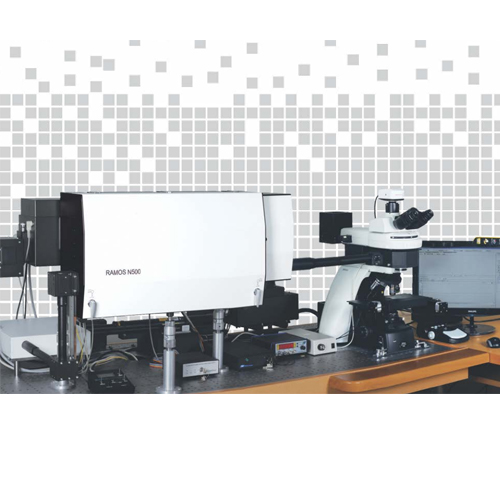
RAMOS N500
3D Scanning Laser Raman Microscope - RAMOS N500
저희 (주)비케이인스트루먼트는 OSTEC사의 공식대리점으로 FTIR, NIR, Raman Spectroscopy 등 다양한 제품을 취급 및 공급하고 있습니다.
RAMOS N500 3D Scanning Laser Raman Microscope

Confocal Laser Scanning Raman Microscope has become a widely recognized research instrument in recent years. Confocal microscopy offers several advantages over conventional wide-field optical microscopy, including the ability to control depth of field, elimination or reduction of background information away from the focal plane and the capability to collect serial optical sections from thick samples. The image of the extended sample is generated by scanning the focused laser beam across a defined area.
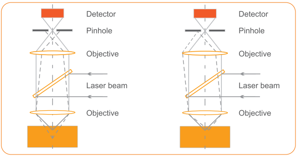
The pinhole aperture rejects the residual scattered rays originated from any out-of-focus points on a sample.


High spatial resolution Raman confocal microscopy can provide information on dopant concentrations and stress distribution in semiconductor materials.
Raman spectroscopy allows easy visualization of cellular components with minimum perturbation.
Confocal Raman spectroscopy allows chemical compounds and molecular conformers in various drugs to be identified and their distribution mapped with high spatial resolution.
Confocal Raman microscopy is an excellent technique for characterization of minerals, detection of components distribution and their phase transitions.
Confocal Raman microspectroscopy is a promising technique which enables measuring the skin care products as well as their penetration capability.
Application areas include identification of unknown substances, different types of fibers, glasses, paints, explosive materials, inks, narcotic and toxic substances, proof of authenticity of x-x-x-x-x-documents.
Confocal Raman offers excellent spatial resolution for characterization of materials (superconductor, polymers, coatings, composites, carbon nanotubes, graphene, etc.).
Raman spectroscopy allows identfication of pigments and binders used in paintings. The spectroscopic analysis of archaeological samples (ceramics, glasses, etc.) provides information on their origin and history. Raman technique allows rapid identfication of colored stones, natural and synthetic diamonds.

Specially designed imaging spectrometer incorporates many features that make it ideal for confocal Raman measurements. The image of pinhole is projected to a multichannel detector without any aberrations.
The smaller amount of illuminated pixels on the CCD matrix leads to the smaller dark counts and the higher spectral resolution.
Spectral resolution of RAMOS N500 with an Echelle grating is 0.25 cm-1.
The 4th order Silicon band at 1940 cm-1 can be observed in less than one minute using a low intensity laser.
2D / 3D images can be acquired rapidly.
People with little or no experience in Raman spectroscopy can use RAMOS N500. The system is highly modular and fully automated. Up to 5 lasers can be used.
The lasers can be switched from one to another by just one click.
Motorized control for laser power, beam diameter, polarization orientation, pinhole size and grating is provided.
Laser Raman microscope RAMOS N500 can achieve:
Laserwavelength, nm | Objective | XY - planeresolution, nm |
| 488 | 100x, NA = 0.9 | 250 |
| 532 | 100x, NA = 0.9 | 275 |
| 633 | 100x, NA = 0.9 | 320 |
| 785 | 100x, NA = 0.9 | 390 |

Laser wavelength, nm | Z (axial) resolution, nm
|
| 488 | 520 |
| 532 | 560 |
| 633 | 660 |
| 785 | 800 |

Laser wavelength, nm | Wavenumber range, cm-1
|
| 325 | 125 - 8000 |
| 355 | 115 - 8000 |
| 473 | 80 - 6000 |
| 532 | 50 - 8000 |
| 633 | 50 - 6000 |
| 785 | 40 - 2800 |
Low-frequency Raman shift measurement range can be expanded using Bragg notch filters.
3D scanning laser confocal Raman microscope RAMOS N500 provides the acquisition of two images within a single scan: a Rayleigh image (using laser light reflected from a sample) and a spectral image by Raman scattering.
Ultrafast imaging option allows to get confocal image in 3 sec (3 μs/pixel).
RAMOS N500 uses fast beam scanning by galvano mirrors.
Layout of galvano mirror scanner module allows mapping with no intensity losses from image center to its edges.

RAMOS N500 system can be used with a number of different detectors.
Up to three detectors can be used simultaneously. Proprietary algorithm for taking high speed of Raman imaging with fast spectral CCD (EMCCD) is offered.
The use of an EMCCD (Electron Multiplying CCD) camera can greatly increase Raman detection efficiency and speed.
Uniform, large size scanning area of a galvanic scanner module:
Automatic XY stage can be used for ultra-wide field imaging.
The panoramic image (hyper image) by automatic stitching of a series of images obtained with the use of galvanic scanner.
RAMOS N500 is equipped with a neon lamp (option) for spectral calibration.
Calibration is possible at any wavelength by one click in the control software.

RAMOS N500 software “Nano SPO” with powerful analytical functionality is designed for hardware operating, data acquisition and data analysis.

SPECIFICATION
*MICROSCOPE, model Nikon Ti | |||
| Type: | inverted | ||
| *Objective lenses: | CFI Plan Fluor 4x, 10x, 20x, 40x, 60x, CF Epi Plan APO 100x | ||
| Stage: | automated | ||
| - travel range: | 114 x 75 mm | ||
| - accuracy (1 mm of translation) / XY repeatability: | 0.06 μm / ± 1 μm | ||
| Z-scanner: | piezo scanner | ||
| - objective translation range: | 80 μm | ||
| - minimal translation step / repeatability: | 50 nm / < 6 nm | ||
OPTICAL-MECHANICAL UNIT (OMU) | |||
| Optimized optics for the spectral range: | 325 - 1100 nm | ||
| Laser radiation delivery: | single, double, triple or penta input port | ||
| Polarizers (excitation and detection channels): | Glan-Taylor prizm, 325 - 1000 nm | ||
| Half-wave plate (λ / 2) positioner: | five-position | ||
| Beam expander: | magnification factor 1 - 4 | ||
| Edge filter positioner: | five-position | ||
| Interference filter positioner: | six-position | ||
| OMU and microscope coupling: | three- or five- position switch | ||
| Spatial resolution: | XY: <300 nm, Z: 600 nm (532 nm laser, 100x, NA = 0.9) | ||
IMAGING MONOCHROMATOR-SPECTROGRAPH MSO 5004i | |||
| Optical configuration: | vertical | ||
| Focal length: | 520 mm | ||
| Ports: | 1 input, 2 output | ||
| Flat field: | 28 x 10 mm | ||
| Grating unit: | 4-position turret | ||
| Grating choice: | 150, 300, 600, 1200, 2400, 3600, l / mm, Echelle (75 l / mm) | ||
| Spectral resolution: | 0.25 cm -1 Echelle grating, wavelength 500 nm) 0.9 cm -1 (1800 I / mm grating) | ||
| Confocal pinhole: | width 0 - 1.5 mm; step size 0.5 μm | ||
| Wavelength accuracy with CCD camera: | 0.005 nm (1800 I / mm grating) | ||
SCANNING UNIT | |||
| Scanning method: | galvanometer scanners of X - Y mirrors | ||
| Scanning speed: | 3 sec (1001 x 1001 pixels, min step 20 nm) | ||
| Scanning region: | 150 μm x 150 μm (using 100x objective lens) | ||
CCD CAMERA FOR SPECTROGRAPH | |||
| Type: | digital CCD camera HS101H | ||
| Sensor: | back-thinned CCD array 2048 x 122 | ||
| Pixel size: | 12 x 12 μm | ||
| Cooling: | Two-stage Peltier cooling with temperature stabilization to -45 °C | ||
| ADC: | 16 bit | ||
CONFOCAL LASER MICROSCOPE UNIT | |||
| Objective positioner: | three-coordinated (X, Y, Z) | ||
| Laser beam attenuator: | VND filter | ||
| Confocal pinhole: | variable from 0 to 1.5 mm, step size 0.5 μm | ||
| Detector: | PMT | ||
LASERS | |||
| The system confi guration allows of using up to 5 lasers: | Power, mW | ||
| Type: | Wavelength, nm | ||
| HeCd laser: | 325 | 10 | |
| HeCd laser: | 441.6 | 50 | |
| DPSS laser: | 473 | 22 | 50 |
| DPSS laser: | 532 | 22 | 50 |
| Helium-neon laser: | 633 | 10 | |
| Semiconductor laser: | 785 | 100 | |
* Microscope, objective lenses, and type of lasers can be offered on customer’s request
Tel +82 (0)42 - 487 - 8240
Fax +82 (0)42 - 488 - 8241
marketing@bkinstruments.co.kr
BKI Bldg., 281-25 Munji-Ro, Yuseong-Gu
Daejeon, 34050, Republic of Korea